• Skip to main content
  • Skip to primary navigation
  • Departments
    • Bioengineering
    • Civil and Environmental Engineering
    • Electrical Engineering and Computer Sciences
    • Industrial Engineering and Operations Research
    • Materials Science and Engineering
    • Mechanical Engineering
    • Nuclear Engineering
    • Aerospace program
    • Engineering Science program
  • News
    • Berkeley Engineer magazine
    • Social media
    • News videos
    • News digest (email)
    • Press kit
  • Events
    • Events calendar
    • Commencement
    • Homecoming
    • Cal Day
    • View from the Top
    • Kuh Lecture Series
    • Minner Lecture
  • College directory
  • For staff & faculty
Berkeley Engineering

CoE Sandbox

Educating leaders. Creating knowledge. Serving society.

  • About
    • Facts & figures
    • Rankings
    • Mission & values
    • Equity & inclusion
    • Voices of Berkeley Engineering
    • Leadership team
    • Milestones
    • Facilities
    • Maps
  • Admissions
    • Undergraduate admissions
    • Graduate admissions
    • New students
    • Visit
    • Maps
    • Admissions events
    • K-12 outreach
  • Academics
    • Undergraduate programs
    • Majors & minors
    • Undergraduate Guide
    • Graduate programs
    • Graduate Guide
    • Innovation & entrepreneurship
    • Kresge Engineering Library
    • International programs
    • Executive education
  • Students
    • New students
    • Advising & counseling
    • ESS programs
    • CAEE academic support
    • Student life
    • Wellness & inclusion
    • Undergraduate Guide
    • > Degree requirements
    • > Policies & procedures
    • Forms & petitions
    • Resources
  • Research & faculty
    • Centers & institutes
    • Undergrad research
    • Faculty
  • Connect
    • Alumni
    • Industry
    • Give
    • Stay in touch
Home > News

Nanotechnology

Schematic illustration of the COF structure, polymer and nanofibrils.

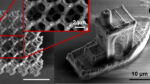
Molecular weaving makes polymer composites stronger without compromising function

03/21/24 — College of Chemistry: New discovery could have a “huge impact on the materials industry”
Transmission electron microscope (TEM) images of the new 2D nanosheet as a barrier coating that self-assembles on a variety of substrates. The TEM experiments were conducted at UC Berkeley’s Electron Microscope Laboratory.

Scaling up nano for sustainable manufacturing

11/08/23 — Berkeley Lab: Scientists, led by Berkeley engineer Ting Xu, have developed multipurpose, recyclable nanosheets for electronics, energy storage, and health and safety applications
Photo of a nanoscale 3D printing benchmarking model called a "3DBenchy" showcases how a new 3D printing technique enabled researchers to embed nitrogen vacancy centers in complex, microscale 3D structures.

Researchers demonstrate new 3D printing technique for quantum sensors

10/31/23 — Innovation may lead to novel applications in precision measurement, biological imaging and environmental monitoring
Photo showing the tops of small, round and rectangular lithium-ion batteries.

Creating a lithium-ion battery for the future

10/05/23 — Unique manganese-based material may pave the way for cheaper, more powerful Li-ion batteries
Schematic portraying heat applied to engineered viruses and the electric charge they emit.

Researchers demonstrate heat-induced pyroelectricity in viruses

09/25/23 — Discovery may pave the way for new bio-inspired devices
Photo illustration of fog on steel nanoengineered mesh used for harvesting and purifying water droplets.

Scientists develop parallel method for fog harvesting and water treatment

08/17/23 — Nanoengineered meshes powered by sunlight work continuously to collect water and remove pollutants
Headshots of Hannah Stuart (left) and Grigory Tikhomirov

Two Berkeley Engineering professors earn NSF CAREER Awards

05/24/23 — Hannah Stuart and Grigory Tikhomirov recognized for research with real-world impact
Image of heteropolymers designed to mimic the properties of natural proteins.

Berkeley engineers develop synthetic polymers that mimic the body’s natural proteins

03/20/23 — Alternative polymers work as well as real proteins and are easier to synthesize, a possible game-changer for biomedical applications
Image of optical nanoscopy, which uses laser beams to strike free electrons, scattering light and providing insights into electron distribution and dynamics within semiconductor materials. (Image courtesy of Laser Thermal Lab/UC Berkeley)

Researchers develop innovative tool for measuring electron dynamics in semiconductors

02/02/23 — Insights may lead to more energy-efficient chips and electronic devices
Photo of Alexander Alvara

ME Ph.D. student takes the road less traveled to UC Berkeley

01/10/23 — Alexander Alvara pushes past life's obstacles and sets his sights on new frontiers in engineering
Frame from video showing that nanoparticle growth is directed not by difference in size, but by defects.

How do nanoparticles grow?

07/27/22 — Berkeley Lab: Atomic-scale movie upends 100-year-old theory, as materials scientists observe nanoparticles ripening in solution at record-breaking resolution
Optical microscopy image of silicon nanowire

New silicon nanowires can really take the heat

05/24/22 — Berkeley Lab: Berkeley researchers show that the new material conducts heat 150% more efficiently, a result that could lead to smaller, faster computer processors
Animation of placement of nanoparticles in a self-assembling material

With a little help, new optical material assembles itself

02/04/22 — Berkeley Lab: Breakthrough by materials scientist Ting Xu and her team could enable large-scale manufacturing of nanomaterials for industry
Electron backscatter diffraction image of titanium.

Stronger, lighter, better

10/21/21 — Berkeley Lab: Research led by Andrew Minor, professor of materials science and engineering, shows sustainable manufacturing potential of nanotwinned titanium
Diagram of microbattery components

Microbatteries that make sense

08/31/21 — Bakar Fellows: EECS professor Kristofer Pister's research shows how embedding batteries on a chip could enable wearable sensors
Hyungjin Kim and Ali Javey

Researchers demonstrate new semiconductor device possibilities using black phosphorus

08/11/21 — Material's "magical" properties under stress and strain could help meet growing demand in optical communications and more
Illustration of single photons approaching metamaterial beam splitter

Berkeley engineers demonstrate unprecedented control of light with a new quantum device

03/15/21 — The at-will control over the behavior of single photons is key to developing optical quantum gates.
3D model of ferroelectric material

Small wonder

11/05/20 — In a breakthrough in the field of ferroelectricity, researchers have made an ultrathin material that powers the smallest of devices with lower amounts of energy.
Michel Maharbiz delivering his TEDMED talk

Using neural dust to eavesdrop on our organs

06/11/20 — In this TEDMED talk, EECS professor Michel Maharbiz describes using extremely miniaturized implants to get a closer look at organs in real time
Royal Society building in London

Materials sciences professor Ramamoorthy Ramesh named to Royal Society

04/29/20 — Ramesh has created nanosized materials that can power small electrical devices with minimal amounts of energy
  • Go to page 1
  • Go to page 2
  • Go to page 3
  • Go to page 4
  • Go to Next Page »
  • Contact
  • Give
  • Privacy
  • UC Berkeley
  • Accessibility
  • Nondiscrimination
  • instagram
  • X logo
  • linkedin
  • facebook
  • youtube
© 2025 UC Regents